Nanoscaled OFETs for circuit applications
Fast organic chips in low-voltage range
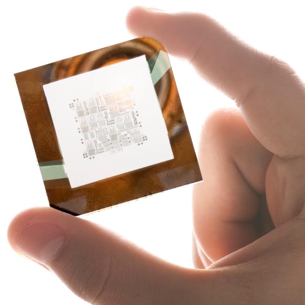
The Institute for Nano and Microelectronic Systems, Institut für Mikroelektronik Stuttgart (IMS CHIPS) and Max Planck Institute for Solid State Research in Stuttgart are currently developing the smallest and fastest organic thin-film transistors (OTFTs) ever having manufactured suitable for industrial application.
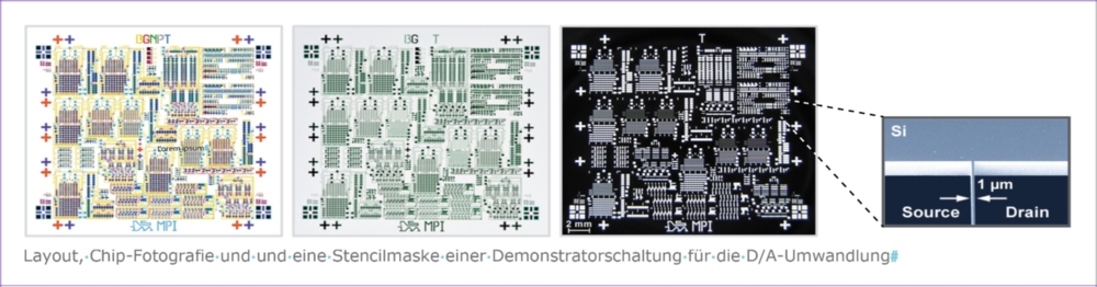
The manufacture is based on high-resolution silicon stencil masks with an outstanding density and stability. This technology enables sub-micron channel lengths and significantly improved transistor matching at better performance for the wiring.
A silicon stencil mask is a thin silicon membrane with etched holes at a predefined geometry. The materials for the circuits are vaporized through these openings and, thus, deposited on a substrate at an equal structure. The masks are created on 150 mm SOI wafers with minimal structures of 0.8 µm and an edge coarseness of less than 50 nm . This causes a prime uniformity of the components and, therefore, enabling certain circuit topologies.
Due to their cost-efficient production OTFTs are considered a fundamental technology for the future manufacture of flexible electronic products in the low-temperature area on light and large-area substrates. This includes flexible displays, intelligent tapes for medical monitoring, bio sensors and other solutions, such as RF-ID tags and smart ticketing as well as smart signage.